Improving EMI/EMC Performance in Multi Layer PCBs
Author : Colby November 06,smt solder paste 2025Table of Contents
If you're looking to enhance the EMI/EMC performance of multi-layer PCBs, you're in the right place. Electromagnetic Interference (EMI) and Electromagnetic Compatibility (EMC) are critical factors in designing reliable and efficient printed circuit boards (PCBs). Poor EMI/EMC performance can lead to signal disruptions, device malfunctions, or failure to meet regulatory standards. In this comprehensive guide, we'll walk you through practical strategies to improve EMI/EMC performance in multi-layer PCBs, ensuring your designs operate smoothly in challenging electromagnetic environments. From grounding techniques to layer stacking, we've got you covered with actionable tips and detailed insights.
What Are EMI and EMC, and Why Do They Matter in PCB Design?
EMI refers to the unwanted electromagnetic energy that can interfere with the operation of electronic devices. EMC, on the other hand, is the ability of a device to function correctly in its electromagnetic environment without causing or suffering from interference. For multi-layer PCBs, which are commonly used in complex, high-speed applications, managing EMI and ensuring EMC are essential to prevent issues like crosstalk, signal degradation, or non-compliance with industry standards such as FCC or CE regulations.
In multi-layer PCBs, the close proximity of traces, high-frequency signals, and multiple power planes can amplify EMI risks. Without proper design considerations, these boards can become sources of interference or fail to operate reliably. By optimizing your design for EMI/EMC performance, you not only improve functionality but also reduce the risk of costly redesigns or failed certifications.
Key Challenges in EMI/EMC Performance for Multi-Layer PCBs
Multi-layer PCBs, often used in high-density and high-speed applications, face unique EMI/EMC challenges. Understanding these issues is the first step toward addressing them effectively:
- High-Frequency Signals:Faster signal speeds, often exceeding 1 GHz in modern designs, generate more electromagnetic noise, increasing EMI risks.
- Crosstalk:With traces packed closely together across multiple layers, unwanted coupling between signals can degrade performance.
- Power Integrity Issues:Inadequate power distribution across layers can lead to voltage fluctuations, contributing to EMI.
- Grounding Problems:Poor grounding can create loops that act as antennas, radiating or picking up interference.
- Regulatory Compliance:Failing to meet EMC standards can delay product launches or result in penalties.
Addressing these challenges requires a systematic approach to design, focusing on layout, component placement, and material selection. Let’s dive into the best practices for improving EMI/EMC performance in multi-layer PCBs.
Best Practices for Improving EMI/EMC Performance in Multi-Layer PCBs
1. Optimize Layer Stack-Up for Signal and Power Integrity
The arrangement of layers in a multi-layer PCB plays a significant role in EMI/EMC performance. A well-designed stack-up minimizes interference by controlling signal return paths and reducing noise coupling.
- Use Dedicated Ground Planes:Place continuous ground planes adjacent to signal layers to provide a low-impedance return path. For a 6-layer PCB, a common stack-up might be Signal-Ground-Power-Power-Ground-Signal. This configuration ensures that signals have a nearby reference plane, reducing loop areas that can radiate EMI.
- Balance Power and Ground Planes:Pair power and ground planes closely together to create a natural decoupling capacitor effect, which helps stabilize voltage and reduce noise. Aim for a separation of less than 10 mils (0.254 mm) between power and ground layers for optimal performance.
- Avoid Splitting Planes:Splitting ground or power planes can disrupt return paths, leading to increased EMI. If splits are necessary, ensure they are minimal and use stitching capacitors to bridge the gaps.
2. Implement Proper Grounding Techniques
Grounding is one of the most critical factors in controlling EMI. A solid grounding strategy minimizes ground loops and provides a stable reference for signals.
- Single-Point vs. Multi-Point Grounding:For low-frequency designs (below 1 MHz), single-point grounding can reduce ground loops. For high-frequency designs, multi-point grounding to a continuous ground plane is more effective in minimizing impedance.
- Ground Vias:Use multiple ground vias to connect ground planes across layers. Place vias close to signal transitions (e.g., layer changes) to maintain a short return path. A via spacing of 0.5 inches or less is often recommended for high-speed designs.
- Avoid Ground Loops:Design your layout to prevent large loops in the ground path, as they can act as antennas for EMI. Keep return paths as short and direct as possible.
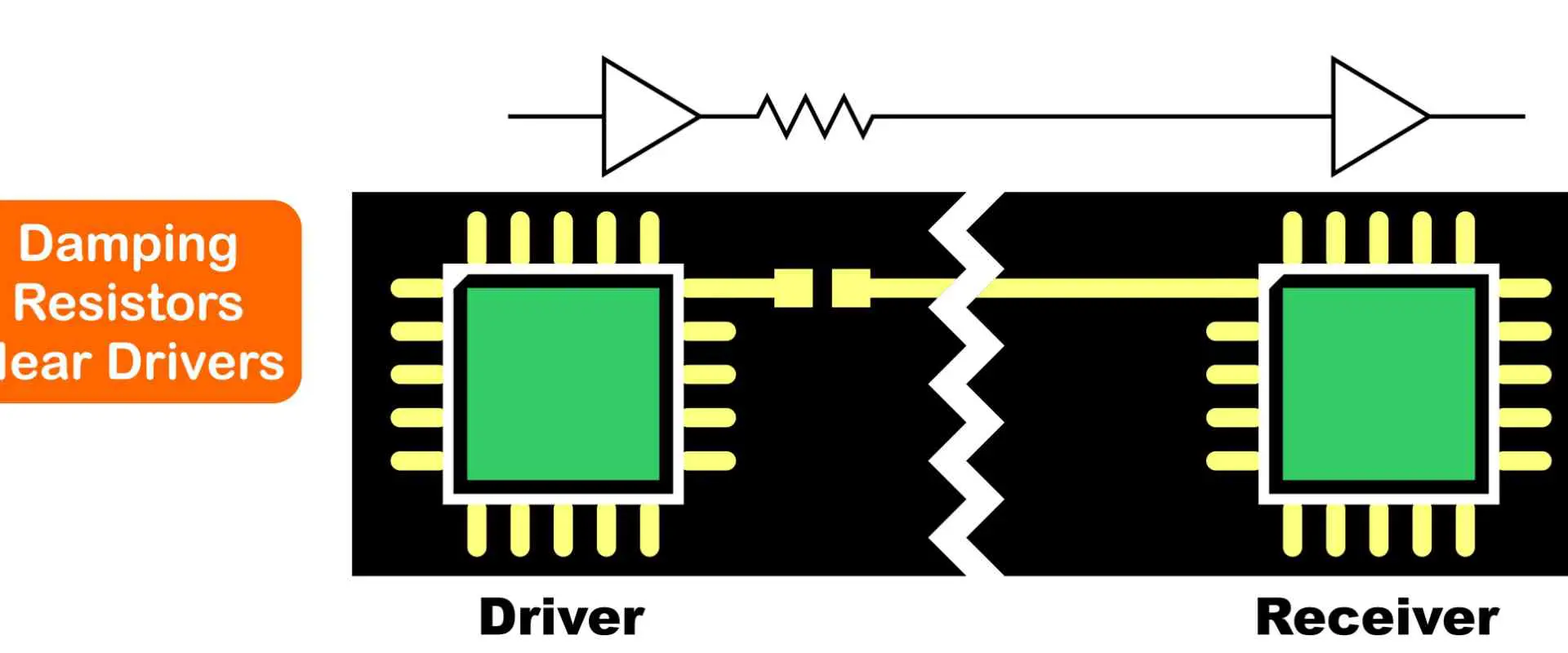
3. Minimize Crosstalk with Trace Spacing and Routing
Crosstalk occurs when signals on adjacent traces interfere with each other, a common issue in multi-layer PCBs with dense layouts. Proper routing and spacing can significantly reduce this problem.
- Maintain Adequate Trace Spacing:Follow the 3W rule, where the spacing between traces is at least three times the width of the trace. For example, if a trace is 5 mils wide, maintain a spacing of 15 mils to minimize coupling.
- Route High-Speed Signals Carefully:Route high-speed signals on inner layers, sandwiched between ground planes, to shield them from external interference. Avoid running high-speed traces near board edges, where they are more susceptible to radiation.
- Use Differential Pairs:For critical high-speed signals, use differential pairs with matched lengths to cancel out common-mode noise, improving EMC.
4. Use Decoupling and Bypass Capacitors Effectively
Decoupling capacitors are essential for stabilizing power supply voltages and reducing noise that contributes to EMI. Proper placement and selection are key to their effectiveness.
- Place Capacitors Close to ICs:Position decoupling capacitors as close as possible to the power pins of integrated circuits (ICs). A distance of less than 100 mils (2.54 mm) is ideal to minimize inductance.
- Choose the Right Capacitor Values:Use a mix of capacitor values (e.g., 0.1 μF and 10 μF) to filter different frequency ranges of noise. Smaller capacitors handle high-frequency noise, while larger ones address low-frequency fluctuations.
- Connect with Short Traces:Use short, wide traces or vias to connect capacitors to power and ground planes, reducing parasitic inductance.
5. Incorporate EMI Filters and Ferrite Beads
EMI filters and ferrite beads can suppress high-frequency noise on power lines, preventing it from spreading across the board or radiating externally.
- Use Ferrite Beads on Power Inputs:Place ferrite beads near the power entry points to block high-frequency noise while allowing DC current to pass. A typical ferrite bead with a current rating of 1A and impedance of 600 ohms at 100 MHz is suitable for many applications.
- Add EMI Filters:For sensitive circuits, consider adding pi-filters (a combination of capacitors and inductors) to further attenuate noise on power lines.
6. Shield Sensitive Components and Areas
Shielding is a direct way to block external interference or contain emissions from specific PCB areas.
- Use Metal Shields:Place metal cans or shields over sensitive components like RF modules to prevent external EMI from affecting them.
- Guard Rings:Surround high-speed or noisy traces with guard rings connected to ground to isolate them from other signals.
- Board-Level Shielding:In extreme cases, consider enclosing the entire PCB in a shielded enclosure if it will operate in a high-EMI environment.
7. Select Materials with EMI/EMC in Mind
The materials used in your PCB can influence its EMI/EMC performance. While standard FR-4 material is common, certain properties should be considered for high-performance designs.
- Dielectric Constant:Choose materials with a stable dielectric constant (Dk) to maintain signal integrity at high frequencies. FR-4 typically has a Dk of 4.5, but for very high-speed designs, consider low-Dk materials like Rogers laminates.
- Thickness:Thinner dielectric layers between power and ground planes enhance capacitance, reducing noise. Aim for a dielectric thickness of 3-5 mils for optimal results.
Testing and Validating EMI/EMC Performance
After implementing these design strategies, testing is crucial to ensure your PCB meets EMI/EMC requirements. Here are the key steps:
- Pre-Compliance Testing:Use near-field probes to measure emissions during the prototype stage. This can identify problem areas before formal testing.
- Formal EMC Testing:Conduct tests in an accredited lab to verify compliance with standards like CISPR or MIL-STD-461. Common tests include radiated and conducted emissions, as well as susceptibility to external interference.
- Iterate Based on Results:If issues are found, analyze the test data to pinpoint sources of EMI and adjust your design accordingly.
Common Mistakes to Avoid in EMI/EMC Design
Even with the best intentions, certain oversights can undermine EMI/EMC performance. Watch out for these pitfalls:
- Ignoring Return Paths:Failing to provide a clear return path for high-speed signals can lead to increased EMI radiation.
- Overloading Power Planes:Distributing too many signals or components on a single power plane can cause voltage drops and noise.
- Poor Component Placement:Placing noisy components (like switching regulators) near sensitive analog circuits can introduce interference.
- Skipping Early Testing:Waiting until the final design stage to test for EMI/EMC can result in expensive redesigns.
Conclusion: Building Better PCBs with EMI/EMC in Mind
Improving EMI/EMC performance in multi-layer PCBs is a multi-faceted process that involves careful planning, precise design, and thorough testing. By optimizing your layer stack-up, implementing robust grounding, minimizing crosstalk, and using shielding or filtering techniques, you can significantly enhance the reliability and compliance of your designs. Remember that every design is unique, so tailor these strategies to your specific application, whether it's a high-speed digital board or an RF circuit.
With the right approach, you can create multi-layer PCBs that not only perform well but also meet stringent regulatory standards. Start applying these tips in your next project to achieve better EMI/EMC performance and ensure your designs stand the test of real-world conditions. For more resources and support in PCB design and manufacturing, trust a reliable partner to bring your ideas to life.
Share · · · ·
The Role of Flux in PCB Wave Soldering: Selection, Application, and Residue Removal
March 16, 2026PCB wave soldering flux types include rosin, water-soluble, and no-clean options with varying activity levels for oxide removal and solder flow. This guide covers selection criteria, spray foam drop-jet application methods, residue removal processes, and alternatives like nitrogen blanketing to boost joint reliability and yields for engineers.
Article
Achieving Uniform Solder Fillets in PCB Wave Soldering: Process Control
March 16, 2026Achieve uniform solder fillets in PCB wave soldering with process control strategies. Optimize flux, preheat, wave height, conveyor speed for consistent fillet shape, height, and wetting balance. Includes visual inspection tips and troubleshooting for reliable through-hole assemblies. Boost quality in production.
Article
Optimizing Conveyor Speed for Efficient PCB Wave Soldering
March 16, 2026Learn PCB wave soldering conveyor speed calculation to manage dwell time, immersion depth, and throughput effectively. Electric engineers get practical steps, best practices, and troubleshooting tips for higher process efficiency and fewer defects in wave soldering operations.
Article
Understanding IPC Standards for PCB Surface Finishes: Ensuring Quality and Compliance
March 11, 2026Understand IPC standards IPC 4552 ENIG and IPC 4553 immersion silver for PCB surface finishes. Ensure compliance, enhance solderability, and prevent common defects to achieve reliable, high quality circuit boards.
Article
Miniaturization Challenges in PCB Assembly
March 11, 2026Navigate the complexities of high density interconnect PCB assembly and precise component placement. Learn to tackle miniaturization challenges, from tiny part handling to thermal stress, ensuring robust and reliable electronics.
Article
High Speed Routing Techniques: PCB
March 11, 2026Master high speed routing in PCBs to ensure signal integrity and minimize electromagnetic interference. Learn essential techniques for robust designs, from controlled impedance to differential pair strategies. Prevent performance issues and achieve reliable electronics.
ArticleGet Instant PCB
Quotations
Full-featured PCB
manufacturing service at low cost.


 相关文章
相关文章


 精彩导读
精彩导读
 热门资讯
热门资讯 关注我们
关注我们